
- ��IC�ؼ���
��ҵ����
- ���֤����

- ��Ա���ͣ���ͨ��Ա
- ����

- �绰��0755-83246479
- �ֻ���13926566652
- ��ַ�������и�����������·�Ѻʹ���A��2901-2906
- ���棺0755-83246479
- E-mail��3106300554@qq.COM
��Ʒ����
- ����IC(7)
- LDO(3)
- ����������(6)
- MOSFET(2)
- ����������(1)
- �źż̵���(1)


��Ʒ��Ϣ
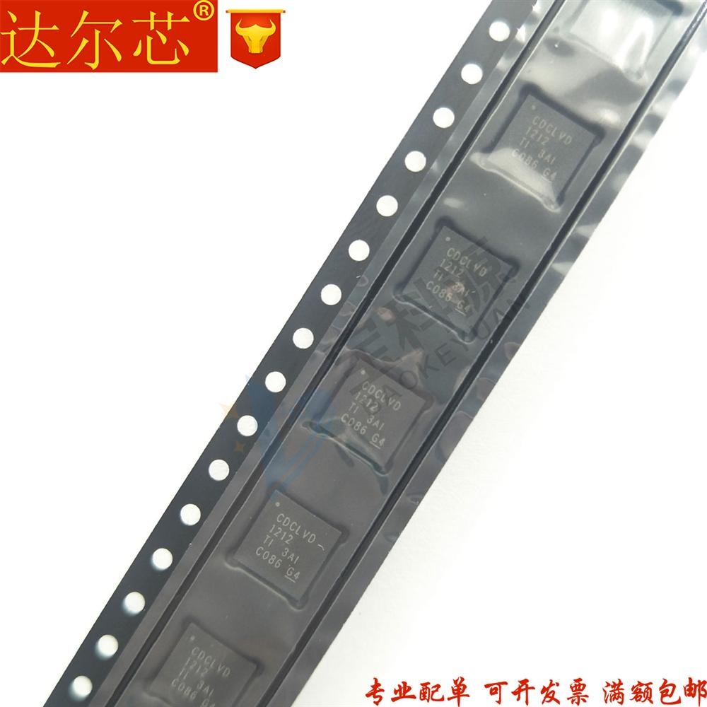
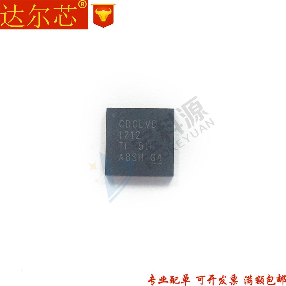
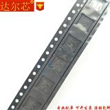
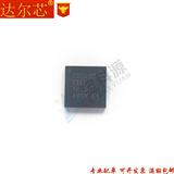
CDCLVD1212RHAR ʱ�Ӻͼ�ʱ��
|
�����б� |
CDCLVD1212RHAR |
|
��� |
���ɵ�·��IC�� |
|
��Ʒ�� |
ʱ��/��ʱ - ʱ�ӻ������������� |
|
ϵ�� |
- |
|
���� |
�ȳ������������䣩����·������ |
|
��·�� |
1 |
|
���� - ����:��� |
2��12 |
|
��� - ����:��� |
��/�� |
|
���� |
LVCMOS��LVDS��LVPECL |
|
��� |
LVDS |
|
Ƶ�� - ֵ |
800MHz |
|
��ѹ - ��Դ |
2.375V ~ 2.625V |
|
�����¶� |
-40��C ~ 85��C |
|
��װ���� |
������װ |
|
��װ/��� |
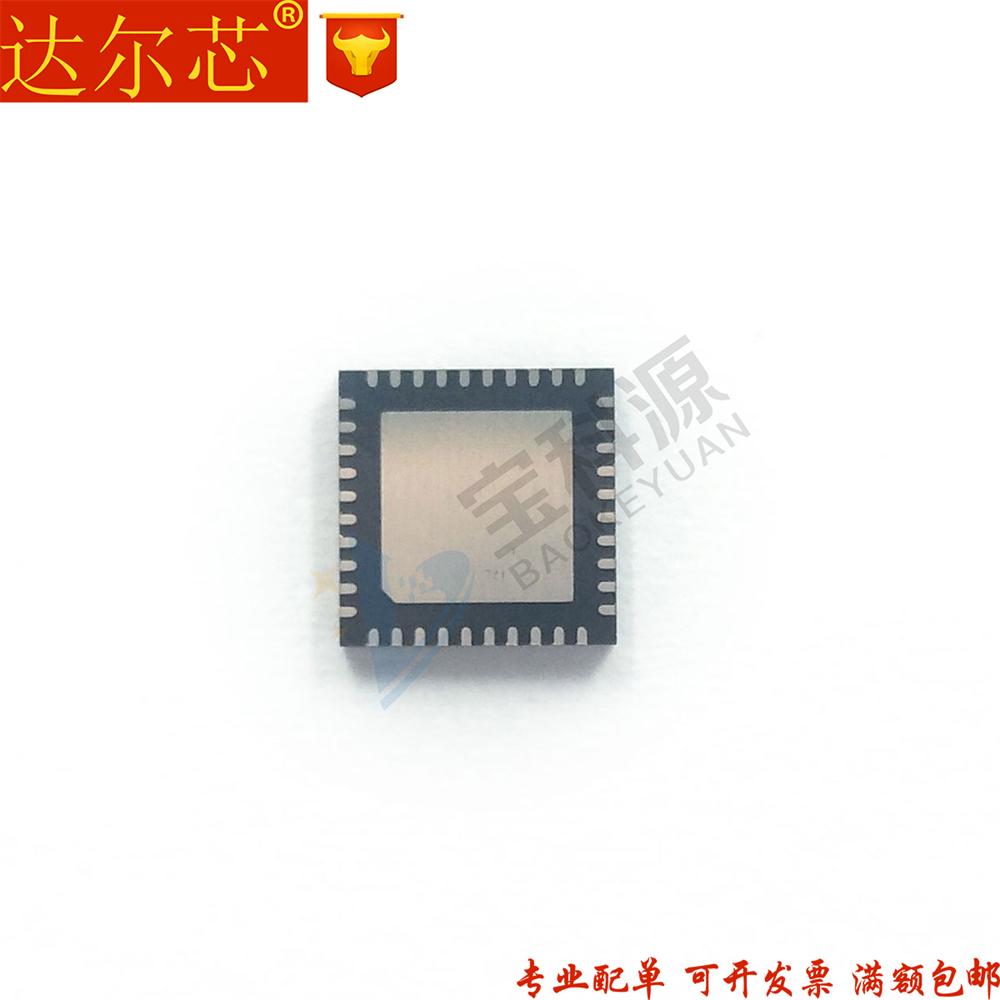
40-VFQFN ��¶���� |
|
��Ӧ��������װ |
40-VQFN��6x6�� |
��˾��Ϊ�ͻ�����13%��ֵ˰��Ʊ��
FEATURES
• 2:12 Differential Buffer DESCRIPTION
• Low Additive Jitter: <300 fs RMS in The CDCLVD1212 clock buffer distributes one of two
10 kHz to 20 MHz selectable clock inputs (IN0, IN1) to 12 pairs of
differential LVDS clock outputs (OUT0, OUT11) with • Low Output Skew of 50 ps (Max) minimum skew for clock distribution. The
• Universal Inputs Accept LVDS, LVPECL, CDCLVD1212 can accept two clock sources into an
LVCMOS input multiplexer. The inputs can either be LVDS,
• Selectable Clock Inputs Through Control Pin LVPECL, or LVCMOS.
• 12 LVDS Outputs, ANSI EIA/TIA-644A Standard The CDCLVD1212 is specifically designed for driving
Compatible 50 �� transmission lines. If driving the inputs in single
ended mode, the appropriate bias voltage (VAC_REF)
• Clock Frequency up to 800 MHz
should be applied to the unused negative input pin.
• 2.375�C2.625 V Device Power Supply
The IN_SEL pin selects the input which is routed to • LVDS Reference Voltage, VAC_REF, Available for
the outputs. If this pin is left open it disables the Capacitive Coupled Inputs outputs (static). The part supports a fail safe function.
• Industrial Temperature Range �C40��C to 85��C It incorporates an input hysteresis, which prevents
• Packaged in 6mm �� 6mm 40-Pin QFN (RHA) random oscillation of the outputs in absence of an
input signal. • ESD Protection Exceeds 3 kV HBM, 1 kV CDM
The device operates in 2.5 V supply environment and
APPLICATIONS is characterized from �C40��C to 85��C (ambient
• Telecommunications/Networking temperature). The CDCLVD1212 is packaged in
small 40-pin, 6mm �� 6mm QFN package. • Medical Imaging
• Test and Measurement Equipment
• Wireless Communications
• General Purpose Clocking